At a junction the surplus electrons of the n-type material diffuse across the junction filling the holes of the p-type material. This process is called combining and forms valence bonds that can no longer diffuse throughout the crystal. This means that in a small area, a depletion region is formed that is free of holes and electrons.
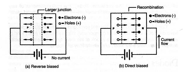
If, in a semiconductor junction, we apply a positive voltage to the n-type part of the junction, it tends to draw electrons out from the n-type material. At the same time, the electrons in the negative side of the power supply fill the holes in the p-type material. The net result is that the depletion region expands to the entire structure of the material. This situation prevents current flow. The diode is now reverse-biased.
If we reversed the applied voltage, the electrons would be forced away from the power supply toward the junction, and, at the same time, holes from the power supply forced to the junction. The electrical force involved in this process compresses the depletion region until it disappears. At this moment, the barrier is broken and the current can flow through the device. With germanium devices this occurs at about 0.2 V and with silicon devices at about 0.6 V. This way the junction is forward-biased.
The device formed by a single p-n junction is called a diode. Figure 1 shows what happens in the two described bias conditions.
The practical semiconductor diode is formed by two pieces of semiconductor materials-n- and p-type germanium or silicon-placed inside an enclosure. The size of the materials is basically determined by the amount of current that they can conduct when forward-biased. Semiconductor diodes operate as one-way roads for the current and are found in a large number of electronic circuits.
Symbol and Types
The diodes are manufactured in different sizes and types according to their applications. Figure 2 shows common diodes and the symbol used to represent this component.
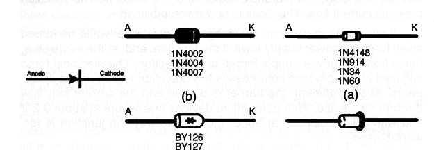
In (a) are germanium and silicon small-signal diodes that are used to handle low currents. In (b) are some rectifier diodes used in circuits where large currents are found.
Diodes are polarized components. Their position in a circuit is important. The identification of the poles is made using several resources. One method is placing the symbol and the component to correspond with the position of the poles and other is to use a strip or ring at the side of the cathode terminal.
Specifications
A. Reverse voltage: Since a diode represents an open circuit when reverse-biased, across the diode appears all the voltage of a circuit. The maximum voltage that a diode can be submitted to without being burned under these conditions is an important parameter to be considered in projects. This voltage is also abbreviated by Vrrm or Vr in data sheets.
B. Direct current: This is the largest current that can flow through the diode when it is fonNard-biased. It is also abbreviated by If.
C. Part number: The most common in real components is the manufacturer specification by a part number. In most parts of America, specifications of diodes are identified by the group “1N” followed by a number. 80, types such as 1N914, 1N4148, and 1N4002 are common.
In European specifications diodes begin with an “A” (for germanium) or “B” (for silicon) followed by a letter. For example, “A” for general- purpose diodes, “Y” for rectifiers, etc. A European part number might look like these: AA115, BA315, BY127, etc. Other manufacturers use proper codes to identify their diodes. Some examples are MR751 and P600D.
Where they are found
The diodes are used basically in functions such as detectors or signal clippers in audio and RF circuits or as rectifiers in power supplies.
As detectors, the reader will find small diodes (silicon or germanium) in radio receivers, TV, remote-control receivers, computers, interfaces, wireless telephones, etc. As signal clippers, the diodes are used to convert an AC into a DC as shown by the diagram in Figure 3.
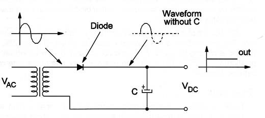
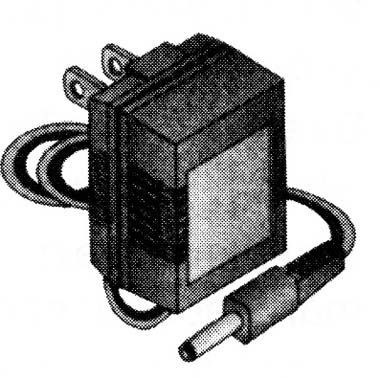
In this circuit, the diode conducts only the positive half-cycles of the AC voltage found in the secondary winding of the transformer. Filtering these positive pulses with a capacitor, a DC voltage can be placed at the output. Power supplies such as this are used to power small DC appliances like calculators, CD players, and transistor radios from the AC power line. Figure 4 shows an AC/DC adapter using an inside circuit like this.
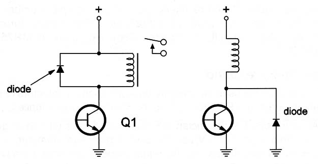
A third case to be included here, and one that is very important to electricians, is the use of a diode to protect semiconductors from voltage spikes generated when inductive loads are triggered. When a relay is open or a solenoid is turned off, it generates a voltage spike strong enough to damage the device used in the control circuit. The energy produced in this process can be absorbed by a diode wired in parallel with the load or with the control device as shown in Figure 5.
Testing
A diode can be tested using a common multimeter or any continuity tester. Adjust the multimeter to a medium resistance scale and place the probes in the diode’s terminals. When biased toward the diode must present a low resistance (between 100 and 5000 Ω) and when reverse-biased a high resistance is read (above 1,000,000 Ω). A diode presenting low resistance when reversed and fonNard-biased is shorted, and the one that presents a high resistance of the two measurements is open. An intermediate read when reverse-biased (between 100,000 and 500,000 Ω) indicates a diode presenting losses.
