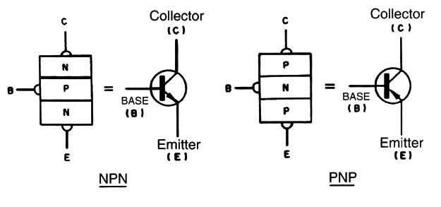
Bipolar transistors are the most important of the semiconductor devices. They are formed by three pieces of semiconductor materials, forming two junctions in the same crystal with a structure such as the one shown in Figure 1.
Although the structure can be compared with two diodes placed back-to-back, the fact that they are in the same crystal means the events occurring at one junction can influence those at the other. The possibility of control makes the transistor one of the most important of all the electronic components.
According to the type of semiconductor, the structures result in two types of transistors-NPN and PNP.
To each piece of semiconductor material, terminals or leads are placed corresponding to the three regions: base (B), emitter (E), and collector (C).
The transistor forms a structure with special electric properties; a current flowing between emitter and collector can be controlled by a current flowing through the base. When connecting the positive pole of a battery to the emitter and the negative to the collector of an NPN transistor, because the two diodes are reverse-biased, no current can flow.
But, if the base-emitter junction is now fonNard-biased in a manner that a small current can flow, this current will cause a high current to flow between collector and emitter as shown in Figure 2.
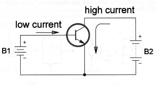
In other words, a small current flowing between the base and the emitter of a transistor can control a large current between collector and emitter. If a 1 mA current through the base causes a collector current of 100 mA, the transistor has a “gain” or “amplification factor” (also called Beta) of 100. This means that the transistor can be used to amplify signals or to act as an electric switch.
Based on the applications, we can find transistors of different sizes and formats with gains ranging from 5 to 10,000. Today there are millions of types of transistors identified by a manufacturer part number. Only with heavy, large “databooks” or “transistor manuals,” could the characteristics of all the main transistors be found.
In applications involving transistors, the use of about 100 or 200 main types with characteristics that are near most of other existing transistors is normal. These transistors can be found easily at a dealer, and in emergency cases, can be replaced with any other.
Symbol and Type
Figure 3 shows the common types of these devices. Notice the arrow in the emitter points outside in the NPN type and inside in the PNP type.
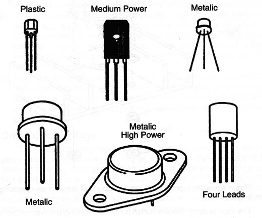
The size of a transistor is determined by the amount of current it can control. Transistors called general-purpose transistors or low-power transistors are small and encapsulated in plastic as shown in (a). Medium-power transistors are shown in (b). These transistors have a hole or another way to place them in heat sinks. ln (e) is a high-power transistor that is mounted in a large heat sink. In (f) is a four-lead transistor. The fourth lead is the case acting as screen.
Figure 4 shows a high-power transistor like the one shown in (c), mounted on a heat sink.
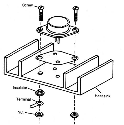
These transistors produce a large amount of heat when operating with large currents.
The main problem the electrician has when working with transistors is the identification of the terminals or leads (emitter, collector, and base).
Many special codes and marks are used for this task such as flat spaces, shafts, marks, color points, and others. With the specific information about one transistor, it is possible to know which terminal does what. Otherwise, using the multimeter is also a possibility to make identification by measuring the resistance between the terminals.
Specifications
Besides the size and type (NPN or PNP), the bipolar transistor can also be classified according to the application. The basic groups according to use are:
A. Low-frequency or audio: Low-frequency or audio transistors are components intended for use in applications where the signals are in the audio band or below some hundreds of kilohertz as in audio amplifiers, power supplies, etc. They can handle low-frequency signals such as the ones found in small amplifiers and the audio stage of radios.
B. High-frequency or RF (Radio Frequency): High-frequency transistors are devices specially intended to operate with signals ranging from some megahertz to gigahertz. They are found in radios, TVs, remote controls, wireless telephones, etc., in the stages where the high-frequency signals are present. They also can be found in sizes according the power to be handled.
C. Switching: Transistors that perform this action are used as switches in high-speed circuits. They are used to turn devices on and off in many applications. They can also appear in low-, medium-, or high-power versions. They are found in inverters, logic circuits, digital instruments, digital controls, etc.
Other specifications
The manufacturers indicate the transistor by a part number. With the part number, a professional can find all the electric characteristics of the device needed to know what it does in a circuit. This is especially important when replacing a transistor because it is possible to find an equivalent or replacement type. The equivalent is a transistor with another part number, either from the same or another manufacturer, but with all the characteristics as the original to replace it in an application.
It is very important to remember that a transistor that is equivalent to another one in application can’t be equivalent in another application or circuit.
The main electrical specifications of a transistor are:
A. Maximum voltages: Vce(max) is the maximum voltage that can be applied between collector and emitter. Vceo(max ) the same, but with open base. Vcb(max) is the maximum voltage that can be applied between collector and base. Vcbo(max) the same, but with open emitter. Veb(max) is the maximum voltage that can be applied between base and emitter. Vebo(max) the same, but with open collector. In some case the absolute values can be specified as Vc, Vb and Ve.
B. Maximum currents: The most important current in a transistor is the collector current. It can be specified as Ic or If (max).
C. Maximum power: When conducting a current, the transistor generates heat that can be transferred to the air. The maximum amount of heat produced by a transistor is given by its maximum dissipation power.These specifications are given in watts. Small transistors dissipate power in the range between 50 and 500 mW. High-power transistors have power specification above 100 W. The parameter is indicated by P or Pd in the datasheets of transistors.
D. Gain: A small current forced to flow by the base element causes a larger current to flow between emitter and collector. The number of times the collector current is larger than the base current is the gain of the transistor or beta factor (B). If a 1 mA current in the base of a transistor causes a 100 mA current between emitter and collector the gain of this transistor is 100. Normally, the transistor has a specification range of gain or minimum gain. For example, the transistor 2N3905 has a gain range between 50 and 150. The gain also can be indicated by a hybrid parameter named hF E, which is equivalent to the beta factor.
E. Transition frequency: The gain of a transistor fails when working with high-speed signals. But, there is a frequency where the gain falls to unit. This means that in this frequency, a variation of 1 mA in base current causes a variation of 1 mA in the collector current, and the transistor cannot operate as an amplifier. The output current is the same as the input current. This frequency is called transition frequency or fT.
Working with transistors
The reader who is not very experienced with electronics sometimes can be confused when working with transistors. Millions of types and too many characteristics to observe when trying to replace one are the main factor of this embarrassing situation. It is even more aggravating when one considers that they have three terminals, not just two as the others.
How are the transistors used? How do you test a transistor? How do you find an equivalent? How do you know how they work? How do you know which is the base, collector, and emitter leads?
As the transistor is one of the most important of the electronic components in any electronic device, more information will be provided on this component later.
How the transistors are used
Figure 5 shows how a transistor is used in the two basic operation modes (linear and saturated). In (a) the load is placed between the power supply and the collector of an NPN transistor.
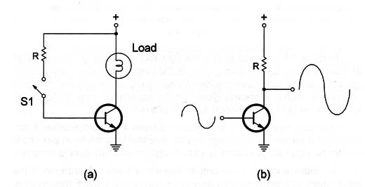
The resistor in the base determines the amount of base current. This resistor is called the biasing resistor. When closing S1 the base current causes the current to flow through the load.
If as shown in (b), a variable current as the correspondent to an audio signal is applied to the base, the small variations of this current will produce large variations in the collector current.
The way the transistors are biased and how the signals to be amplified can be applied and taken off a circuit determine three basic configurations of the transistors. The three ways or basic configurations are shown in Figure 6.
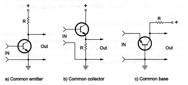
In (a) is the common emitter configuration presenting larger voltage and current gain (power gain), in (b) is the common emitter configuration giving a high current gain but low-voltage gain, and in (c) the common base configuration is shown. Based on the application, one configuration can have the best performance and is preferred.
Normally, more than one transistor is used in any application. Each transistor is the center of a stage and the amplified signals must pass from one to the other stages being amplified until the desired level is reached.
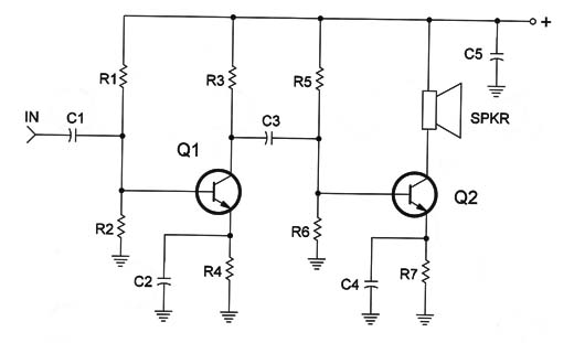
An audio amplifier, for example, has many stages. Starting from the point where the preamplifier takes the weak signal from a microphone, passing it to intermediate amplification stages, and ending in a power output stage, it can source enough power to drive a loudspeaker reproducing sound with a desired volume. Figure 7 shows a typical circuit of an audio amplifier using two transistors.
The way the transistor transfers the signals from one stage to another is called coupling, and there are several coupling methods as shown in Figure 8.
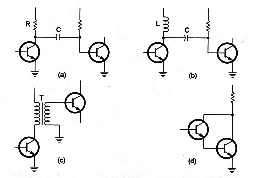
In (a) is an RC coupling. The signal is transferred from one transistor to another by a capacitor. In (b) is an LC coupling. The capacitor is also used to transfer the signal from one stage to another. In (c) is a transformer coupling, and in (d) is the direct coupling. A special method of direct coupling, called a Darlington coupling (not shown), is when two NPN or PNP transistors are used.
Testing and identification
The reader who is just starting with electronics may find some appliances using transistors that are in trouble. How should one proceed in this case?
Transistors are found practically in all equipment, forming the central element of many stages. Each stage can have as core one or more transistors in one of the configurations we have seen before. The main test that the electrician can do is measuring the voltages in the leads of the transistor using a multimeter.
As a general rule, the collector voltage is higher than the emitter voltage in an NPN transistor and the inverse in a PNP transistor as shown in Figure 9.
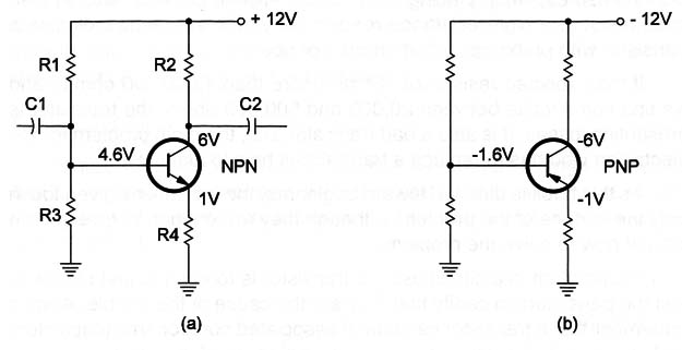
The base voltage is 0.6 V to 0.7 V above the emitter voltage in an NPN silicon transistor and the same below the emitter voltage in a PNP silicon transistor. ln old germanium transistors the difference is 0.2 V. If the voltages are different, the biasing resistor or other elements surrounding the transistors can have problems.
The static test of a transistor or the test out from a circuit, is done by measuring the resistance between the elements (EBC) using a multimeter. It is a “junction test” where it is verified whether the two junctions (base-emitter and base-collector) are okay.
The basic test consists of “seeing” if the two “virtual” diodes corresponding to the two junctions are good. Simply adjust a multimeter to a low-resistance scale and make six measurements in on the transistor to test it. Figure 10 shows how to do these measurements.
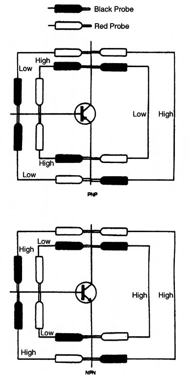
When placing the probes between base/collector and base/emitter one measure must be of a high resistance and the other a low resistance.
Both measures, when placing the probes between collector and emitter, must result in a high-resistance reading. Any different result indicates a transistor with problems, either shorted or open.
If the expected resistance is high (more than 1,000,000 Ω), and we find some value between 20,000 and 500,000 Ω, the transistor is presenting losses. It is also a bad transistor. But, the main problem for the electrician who has to replace a transistor is how to identify it.
As this article is directed toward beginners, the indications given touch only the surface of the problem, although they are enough to give you an idea of how to solve the problem.
If a problem in a circuit using a transistor is found, the first step is to test the transistors to certify that they are the cause of the trouble. Always remember that a transistor can burn if associated components (capacitors and resistors) fail. A capacitor, in short, can cause high currents across a circuit burning a transistor. 80, before replacing a burned transistor, test all the components near it as well.
For the replacement, if the original cannot be found, look in a handbook for equivalencies, replacement types, or the characteristics. As a practical rule, a transistor for the same function (small signal for instance) and the same type (NPN or PNP) with the same or greater gain, the same or greater Vce, and the same or greater collector current (lc), can be used as replacement. In some critical applications such as high-frequency circuits, the fT (transition frequency) must be equal or higher.
