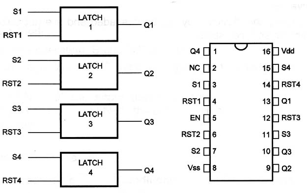
Description: This package contains four independent NAND Fi/S latches With tri-state outputs. The third state is controlled by a common EN pin.
Functional Diagram and/or Package:

Pin Names:
Vdd - Positive Supply Voltage [BV to 15V]
Vss - Ground
EN - Enable
S1, S2, S3, 54 - Set
RST1, RST2, RST3, RST4 - Reset
Q1, Q2, Q3, Q4 - Outputs
NC - Not Connected
Truth Table:

Operation Mode:
S and RST are normally “1’1
When S goes to “0” Q passes to “1” and maintains the logic level.
When RST goes to “0, Q passes to “0” and stays in this state.
S and RST can't be “0” at the same time because both outputs pass to “0. This is a disallowed state.
EN controls the tri-state function. The outputs go to the third state When EN=D.
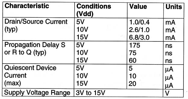
Electrical Characteristics:

Other Devices:
The 4043 is similar, but it has NOR inputs.
Applications:
Holding Registers [for Multiregister Systems]
Strobed Registers
Four Bits of Independent Storage
Digital Logic
Observations:
Do not cascade this device or use as shift register.


