-
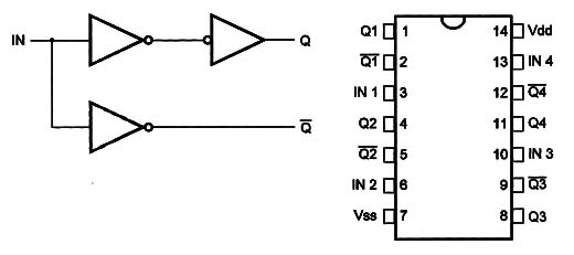
Description: This package contains four true/complement buffers consisting of N and P channel transistor having low channel resistance and high current capability.
-
-
Functional Diagram and/or Package:
-
-

-
-
Pin Names:
-
Vdd - Positive Supply Voltage [3V to 15V]
-
Vss - Ground
-
lN1, IN2, IN3, IN4 - Inputs
-
Q1, Q2, Q3, Q4 - True Outputs
-
Q1/, Q2/, Q3/, Q4/ - Complement Outputs
-
-
Truth Table:
IN Q Q/ 0 1 0 1 0 1 -
-
-
Operation Mode:
-
The output of one buffer/inverter is appiied to the input of the other buffer.
-
The logic level applied to the input of the hiooig appears “inverted in the first output and inverted again [true] in the. second output. A “1” in the input causes to a “0” to appear in the first output and a “1” in the second output.
-
-
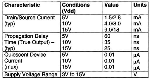
Electrical Characteristics:
-
-

-
-
Other Devices:
-
The 4669 and 4050 can be used in the same function.
-
-
Applications:
-
High Current Driver [sink and source]
-
CMOS-to-TTL Driver
-
Display Driver
-
Digital Amplifier
-
Transmission Line Driver
-
-
Observations:
-
This device is TTL compatible.
-


