Description:
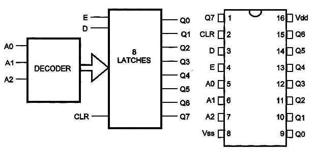
8 bits can be addressed from three address inputs using the circuit inside this package.
Functional Diagram and/or Package:

Pin Names:
Vdd - Positive Supply Voltage (3V to 15V]
Vss - Ground
Q0 to Q7 - Outputs
D - Data Input
CLR - Clear
A0, A1, A2 - Address Inputs
E – Enable
Truth Table:

Operation Mode:
Data enters by a particular bit in the latch when addressed by inputs A0, A1, and A2 and when E is “0”.
When E is “1", data entry is inhibited.
Outputs can be read independently of the E state at any time.
If CLR = 1 and E = 1 all the bits are reset to “0”.
If CLR =1 and E =0 the devices act as a 1-of-8 Demultiplexer. The bit addressed has an active output that follows the data input. The others are kept in “0”
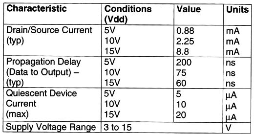
Electrical Characteristics:

Applications:
Data Converters (Seriel-to-Parallel)
Remote Control Holding Register
General Purpose Register


