

Description:
This device Contains four separated shift register sections two sections of four stages and two sections of five stages. Each section has an independent data input. The outputs are found in the fourth and fifth stage of each section. The device uses a common clock input for all stages.
Functional Diagram or/and Package:
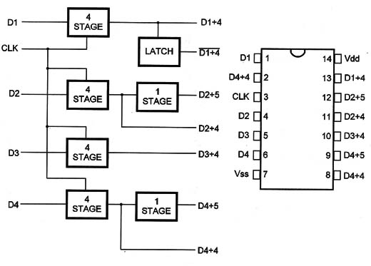
Pin Names:
Vdd - Positive Supply Voltage (3 V to 15 V]
Vss - Ground
D1+4, D1+4, D2+5, D3+4, D4+5 - Outputs
D1, D2, D3, D4 - Inputs CLK – Clock
Truth Table:
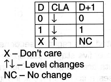
Operation Mode:
A common clock signal is used for all stages. Data is shifted to the next stage on the negative transition of the clock. Through programmed connections of inputs and outputs, multiple register sections of 4, 5, 8, and 9 stages or single sections of 10, 12, 13, 14, 16, 17, and ’IB stages can be implemented using one of these devices.
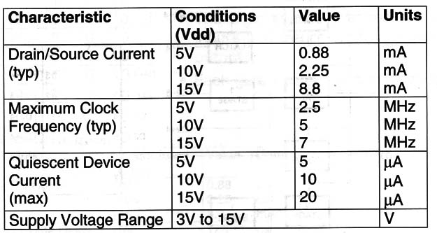
Electrical Characteristics
Applications:
Shift registers [serial]
Time delay applications
Frequency division
Observations:
This device has a low clock input capacitance 6 pF.


