Translation into English:Patricia Lima Carlos
The simplest way to control a higher current load using a small current is through a bipolar transistor. You can also use other types of transistors such as power MOSFETs and IGBTs, but this is not the focus of this article.
The reader interested in knowing more about the operation of a bipolar transistor (NPN or PNP) can consult our Electronic Course (Basic Electronics) in the form of a more complete book or on the website soon available for free.
But to make it easier to understand how we can use a transistor to control power loads from the signals of a microcontroller, we give a summary.
The bipolar transistor
Three pieces of semiconductor materials of different polarity P and N, such as the germanium and the currently most used, silicon, are placed alternately, as shown in Figure 1.
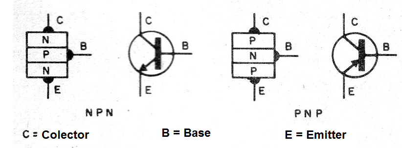
Since we have two possible arrangements, there are two types of transistors given by the polarities of the materials: NPN and PNP.
As shown in the figure the symbols are different (arrow out on the NPN and inward arrow on the PNP) and the terminals are given the names of emitter, collector and base.
The two types of transistors can be used basically according to the circuits shown in Figure 2.
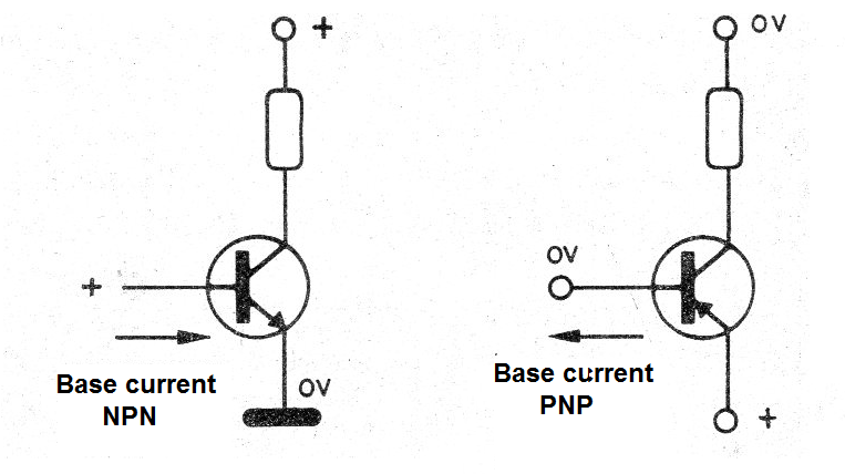
The circuit to be controlled, called "load", is usually connected to the collector and the control signal is applied to the base.
In the case of a microcontroller, the base current comes from the outputs of the microcontroller while the load may be a motor, a solenoid, a lamp or a complete circuit, for example a siren or an inverter which generates high voltage.
This signal, as shown in the same figure, consists of a weak current which will be amplified by the transistor.
Thus, if a transistor has a gain of 100, it means that it can increase by 100 times this current.
With an 1 mA current, we will then be able to control a 100 mA load.
If what we apply at the base of the transistor is an audio signal, for example, the sound of a microphone, it will be amplified 100 times.
In the case of a microcontroller, we can avoid its overload by operating a 1 A motor with a current of its output of only 10 mA.
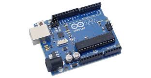
Note that an Arduino supplies 40 mA at 5 V and 50mA at 3 V. This does not mean that we can drive several loads with this current at the same time without overloading its circuitry, even causing a problem.
We can work more "light” and even power loads which operate at higher voltages such as 6, 9, 12 V or even more if a transistor is used.
In fact, there are microcontrollers which have much lower voltage outputs, such as 1.8 V and being powered by small "type" button cells, their current supply capacity is insufficient to power almost any type of current load above 10 mA.
Shields using transistors with separate batteries are indispensable in these cases.
See the current directions to the different for the NPN and PNP transistors.
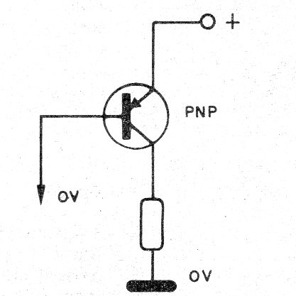
We can control a circuit with a PNP transistor simply by grounding its base, as shown in Figure 4.
As a control shield, the transistor will not be used to amplify audio signals which vary within a continuous range of values. It should be used to turn a load on or off, i.e., as a key.
The Transistor as a Switch
The first circuit we present, given in figure 5, shows how to use a transistor as a switch.
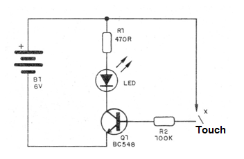
When there is no current at the base of the transistor, it remains "off", that is, there is no current flowing between its collector and its emitter.
The load is disabled and in our case the LED remains off.
If we connect the X points by touching one wire on the other or on the point indicated on the terminal bridge, a current flows through the base of the transistor and it "switches on", causing the LED to light up.
See Figure 6 how to assemble this circuit in a protoboard.
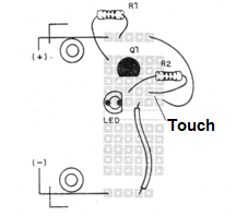
The reader can then realize that when we use the transistor, it operates as a key, it must be polarized in the region of saturation (commutation).
In order to the reader to have an idea of ??how the components of this step should be sized, let's give a practical example of design.
Design of a Shield with a Bipolar Transistor
We describe below the procedures for calculating a switching stage with a transistor driving a direct current load. The fact that the transistor operates saturated in this type of circuit requires a special calculation procedure, different from what happens when we work with the transistor in its linear region.
The configuration analyzed is precisely one of the most used in our practical projects involving microcontrollers, digital circuits, automation circuits and others.
Let us first recall that when we use a transistor to excite a direct current load, such as an indicator light, a relay, an LED, or even a solenoid, the calculations are basically summarized in determining the basic resistor as a function of gain of the used transistor.
However, how to accurately calculate this resistor is something with which the assemblers usually find some difficulty.
Operating saturated, the transistor behaves differently than it does in its operation in the linear region when it amplifies signals. This leads to the procedures we describe below.
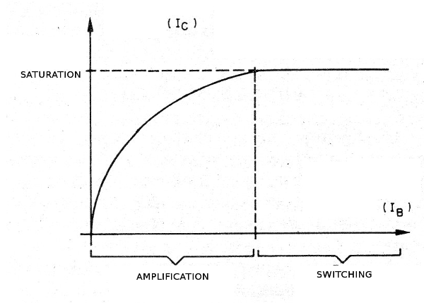
Operation as a switch
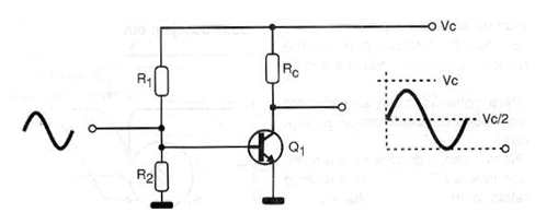
When a transistor operates as an amplifier it is assumed that base current variations cause larger variations in the collector current (in the common emitter configuration, for example), which means that it must have "space" to respond to these variations.
This means that, as shown in Figure 8, it must be polarized so that it is "half conducting" and, with this, the collector voltage remains at a value which allows its variation to be more or less, following the signal. This corresponds to a polarization more or less in the middle of the load line.
On the other hand, when the transistor operates saturated, it conducts or does not conduct, which means that at one moment it conducts, and at the other it does not, which leads to its operation at the ends of the load line.
The voltages appearing on the electrodes in the two conditions are different,
as shown in Figure 9.
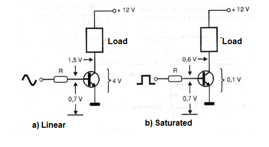
In linear mode, the collector voltage is usually somewhat high, depending only on the region of the charge line to which it is polarized. On the other hand, when it operates saturated, the voltage between the collector and emitter drops almost to zero when it drives.
This means that while in the blocking condition practically no current flows through the transistor, when it is saturated and the load receives the full power, we have the maximum currents. In the design of such stage, we need to take into account some important factors such as:
a) The current which the load requires, if it is within what the transistor can provide.
b) If the gain of the transistor is sufficient to supply the load current from the current available at the input.
c) If the power dissipated by the transistor when conducting the maximum current is in accordance to its dissipation capacity.
Formulas
To calculate the various elements of the circuit, we need to use two sets of formulas which correspond exactly to the blocking and saturation conditions of the circuit. We take the circuit of Figure 10 as a reference for the various quantities involved:
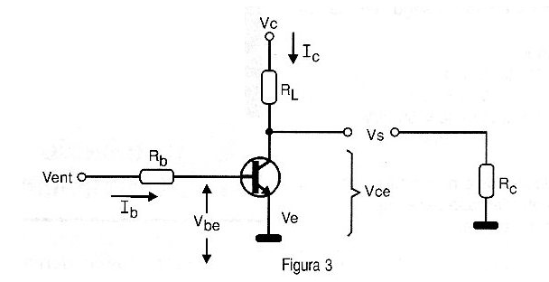
a) Blocking
Ve = 0
Ic = 0
Vs =
Vc
( RL )
Rc + RL
Where:
Ve is the voltage of the transistor emitter in volts (V)
Ic is the collector current in amperes (A)
Vs is the output voltage at (V)
Rc and RL are the load resistors in ohms (?)
b) Saturation:
Ib >
Ic
hfe
Ib =
Ve – Vbe
Rb
Ic =
Vc – Vce(sat)
Rc
Where:
Ib is the base current in amperes (A)
hfe is the static current gain of the transistor
Ic is the collector current in amperes (A)
Ve is the emitter voltage in volts (V)
Vbe is the voltage between the base and the emitter in volts (V)
Vc is the collector voltage in volts (V)
Vce (sat) is the saturation voltage between the collector and the emitter
Rc is the load resistance in ohms (ohms)
In practice we use Vs = Vce (sat) = 0.25 V
On the other hand, the base current is always chosen being greater than the calculated one, in order to guarantee the saturation of the transistor. Factors of 2 to 4 times can be adopted in practical projects.
Taking these factors into account, we can take a practical example of calculation.
Project Example
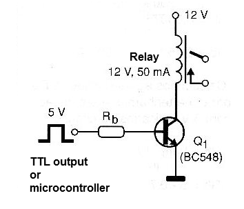
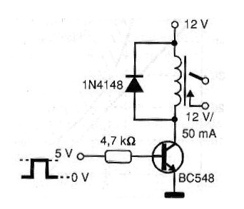
We wish to calculate the components for a shield circuit of a load of 50 mA (a relay, for example) with 12 V from the signal obtained of a TTL (5 V) output or from a microcontroller. The circuit is shown in Figure 11. The adopted transistor is the BC548, which has the following characteristics:
We start from the characteristic curve of this transistor in which we draw the load line (assuming Vce = 0) and which is shown in Figure 12.
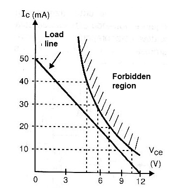
Note that this line is totally below the "forbidden" region where the dissipation of the transistor rises from the limits admitted by the component, which can then be burned.
We then have the following data for calculation.
a) Cut: Ic = 0
Vce = 12 V
b) Saturation Ic = 50 mA
Vce = 0 V
1. We first calculate the base current for the transistor to saturate:
Ib >
3 x
Ic
hfe
Ib =
3 x
0.05
200
ib = 0,00075
Ib = 0,75 mA ou 75 MA
2. We now calculate the value of Rb so that we have the saturation with 5 V applied to the circuit.
Rb =
Vent – Vbe
Ib
Rb =
5 – 0,7
0,75
Rb = 5,73k ohm
In practice, we can adopt both 5.6k ohm and 4.7k ohm, which gives us even greater current of saturation.
In Figure 13 we have the complete circuit.
Conclusion
This is a fairly simple configuration, since it is a DC circuit that has only two states. However, the use of components with correct values ??is extremely important to ensure the proper functioning of the circuit. The reader, who is doing a project involving this type of stage, should be prepared so as not to have surprises.
In our website we have hundreds of practical digital circuits or involving microcontrollers which use stages or shields like this.
When working with your microcontroller, keep these calculations in mind and use them if you are doing a graduation work, so your report is complete.
We remind you that the content of our articles is completely free and that everyone can use them at their will as long as you indicate the source (author, site and date).
This article was originally written in 2009 and updated in 2017 with a content extension and new concepts.
We also inform you that in our books "Circuit Bench” we have several editions dealing exclusively with shields, in addition to a large number of them in the section "Circuit bench".
