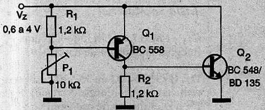
The circuit shown in Figure 1 has a certain degree of sophistication with respect to a common zener but it can be set with a certain precision and is capable of handling currents up to 100 mA.

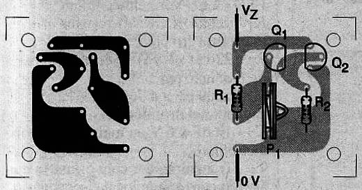
Its assembly can be done on a small printed circuit board as shown in Figure 2.

The zener voltage of this circuit simulator can be adjusted between 0.6 and 4 V typically. Higher voltages can be obtained by changing the value of R1 and R2.
The transistor Q2 should be mounted on a small heatsink, especially if the circuit operating at maximum current capacity, and where an medium power transistor BD is used.
We note that although simulating a zener diode linearity of the circuit is not as good as that of a real component. Thus, the zener set voltage may vary substantially with changes in input voltage and current in the circuit itself. For greater accuracy in the common trimpot adjustment may be replaced by a multi-turn type.
We also observed that the zener diode can also be simulated "reverse" manner with the use of an NPN transistor for Q1 (BC548, for example) for Q2 and a PNP (BD136, for example).
Q1 - BC558 – General Purpose PNP transistor
Q2 - BC548 or BD135 – General purpose NPNTransistor (up to 50 mA) or medium power (up to 100 mA)
R1, R2 -1.2 k Ω x 1/8 W - resistor - brown, red, red
P1 - 10K Ω - trimpot
Miscellaneous:
Printed circuit board, heat radiator for Q2 (if necessary), wire, welding, etc.


