Among the applications for the 4093 IC we will highlight the ones related to digital signal amplification and drive power circuits such as in shields.
Digital Amplifiers and Buffers
A high-impedance digital signal applied to the input of a 4093 gate wired as an inverter results in a low-impedance digital signal. The output signal has the same waveform but this is valid only with digital signals as the square waveforms shown in Fig. 1.
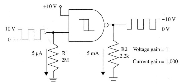
We can consider this configuration to be a unity-gain voltage amplifier, but a high-current-gain amplifier. This circuit can be used in several practical application, as will see in the following pages. For instance, a digital amplifier can be used to drive powerful loads with weak digital signals, as shown in Fig. 2.
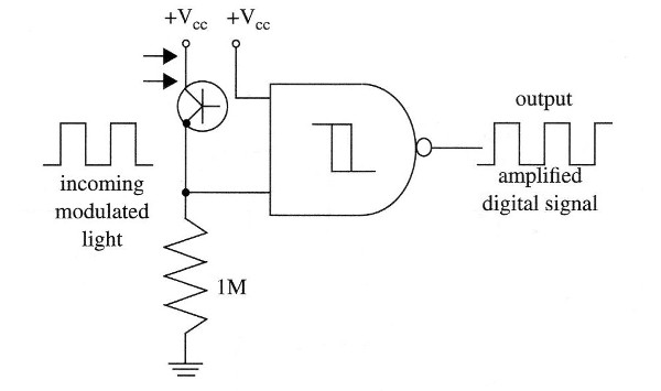
Note that this an inverter configuration, so the output is a 1 when the input is a 0, and vice versa. A phase-shift is added to the amplífied signal.
This circuit can also be used to isolate an oscillator or other input-circuit from an output, as shown in Fig. 3.
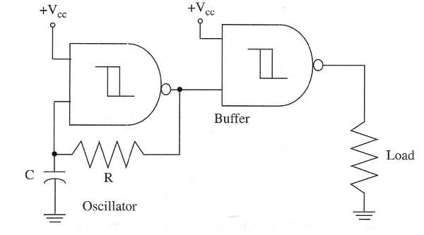
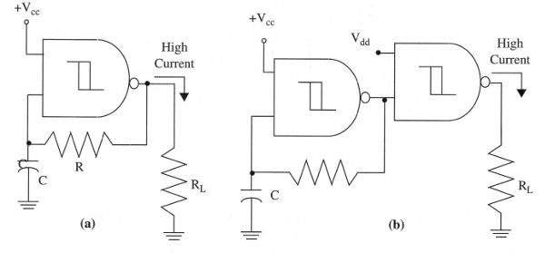
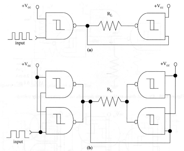
If we connect a heavy load to the output, as shown in Fig. 4a, the oscillator will show erratic-operation. This problem can be solved with a buffer, as shown in Fig. 4b.
Outputs
What a 4093 IC output can drive is an important consideration to the experimenter who wants to make his own project. CMOS integrated circuits such as the 4093 have low output capability. Even with a 10 V power supply, each gate cannot source or sink more than a few milliamperes, as suggested in Fig. 5.
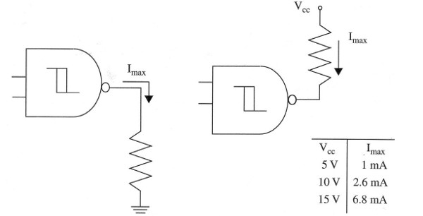
Only light loads as LEDs, piezoelectric transducers, crystal earphones, can be driven directly by these outputs. To get more power from CMOS integrated circuits, we have to employ some special circuits. For example, if your project does not use all the 4093s gates, you can connect the unoccupied gates to give extra power to the load. Connect the gates in parallel as shown in Fig. 6.
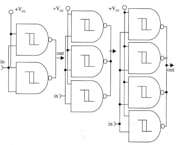
We have twice the maximum current using two gates, and with three gates we can get three times the maximum current. Using a 10 V power supply, you can source or sink about 10 mA with these circuits.
More power can be applied to the loads with a push-pull stage, as shown in Fig. 7. Two or four gates can be used to drive audio loads with currents up to some tens of milliamperes.
However, if you want to drive more powerful loads, such as loudspeakers, relays, lamps, and so on, you need much more power, and this implies that special output stages be used. Transistors are suitable components for this task.
Figure 8 shows two output stages that can be used to drive loads with current requirements up to 100 mA. The circuit shown in Fig. 8a uses an NPN transistor. The transistor in this circuit is biased to conduct when the gate is at 1 logic level. The circuit shown in Fig. 8b uses a PNP transistor and is biased to conduct with a 0 in the gate output.
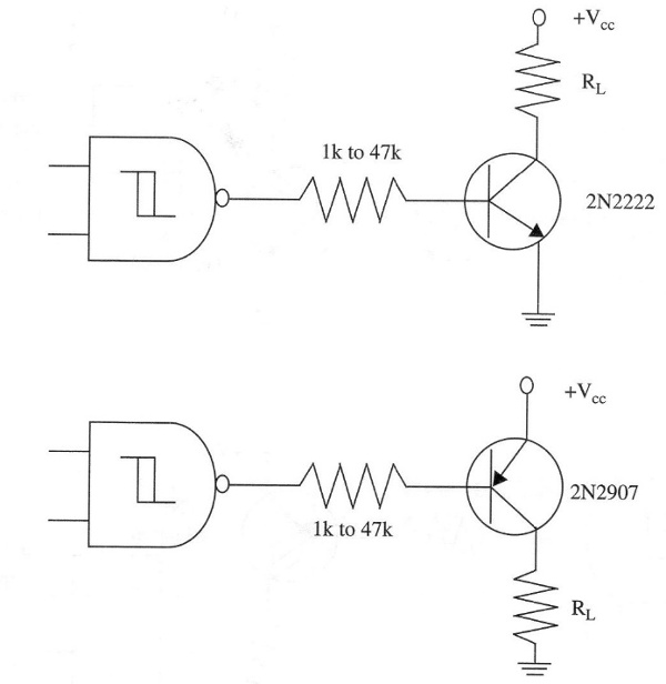
With small-signal transistors and audio transducers, we can get powers ranging from milliwatts to hundreds of milliwatts. The load impedance can range from 4 to 80 ohm, depending on the power supply voltage and the application.
With a 12 V power supply and low-impedance loads, medium power transistors should be used, such as the 2N2218, BD135, and TIP31 (all NPN), or the BD136 and TIP32 (all PNP). These transistors must be mounted on heatsinks. The output currents can be raised to 1 A in these circuits.
To get much more power without loading the ICs output, we can also use a Darlington transistor. Darlington transistors with current gains ranging from 800 to 10,000 are common. The circuits are shown in Fig. 9.
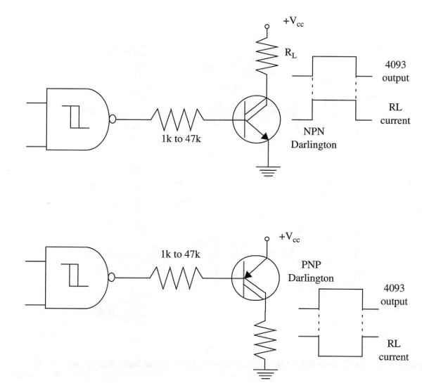
TIP120, TIP121, and TIP122 (NPN), and TIP115, TIP116, and TIP117 (PNP) devices are suitable for this application. These transistors can supply loads with currents up to 3 A and must be mounted on heatsinks.
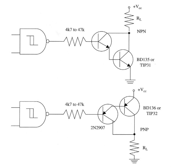
A Darlington pair can be improvised with two common transistors, as shown in Fig. 10. The total current gain for this configuration is given by the first transistor gain x the second transistor gain. Typical base-resistor values are in the range of 1 to 47k ohm.
Complementary pairs (an NPN and a PNP transistor with the same current-gain and other characteristics) can also be used to drive a low frequency load with high power, as we show in Fig. 11.
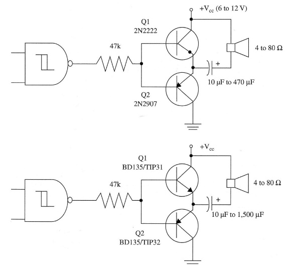
Figure 11a shows a low-power complementary output stage with small signal transistors supplying some hundreds of milliwatts to a loudspeaker. More power is given by the output stage shown in Fig. 11b. Medium- power transistors are used with a 12 V power-supply.
The 4093 IC outputs can also drive SCRs and triacs. Sensitive SCRs, such as the TIC 106, can be triggered directly with the output signals. In the circuit suggested in Fig. 12, the SCR goes on with a high level in the CMOS output.
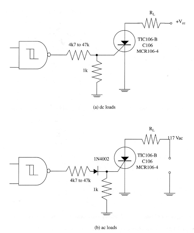
Triacs and less sensitive SCRs can be triggered with boosted signals, as shown in Fig. 13. Transistors are used to get more trigger current. The resistor value depends on the trigger requirements and the applications intended for the circuit. The BD135 can replace the 2N2222.
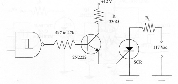
Finally, you can also use power FETs to get high power outputs from the 4093 IC. A configuration used to drive do loads with current drain up to 10 A is shown in Fig. 14.
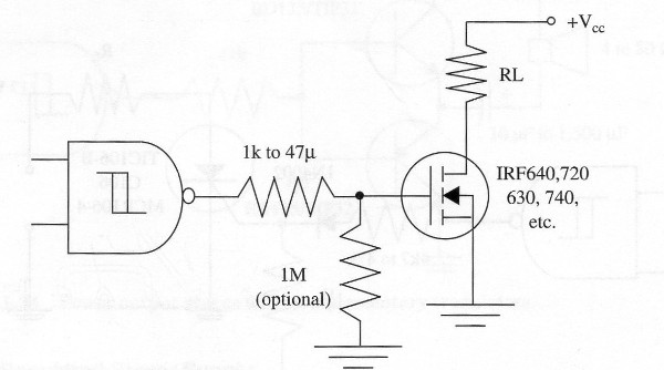
The current drain of this configuration depends upon the power FET characteristics. Power FETs rated to drain currents up to 10 A are common and can be used in many applications described in this book. Types such as IRF640, IRF720, and others of the series IRF can replace the TIP Darlington and common transistors in almost all of the projects described in this book to get better performance.
Important in all these stages is that the voltage that power the stage can be different from the voltage used to power the 4093.
So, we can use the 4093 in a shield for microcontroller powering it from a 3,3 or 5 V supply and drive the stage using common transistors, Darlingtons, SCRs Triacs or MOSFETs with higher voltages, 12 to the AC power line.
