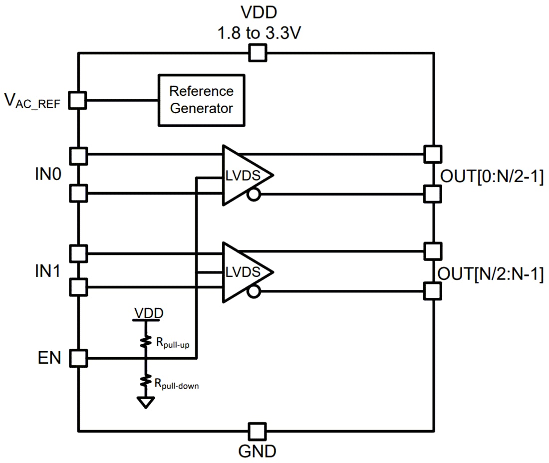
Texas Instruments LMK1D210x Low Additive Jitter LVDS Buffer distributes two clock inputs (IN0 and IN1) to a total of up to 8 pairs of differential LVDS clock outputs (OUT0, OUT7) with minimum skew for clock distribution. Each buffer block consists of one input and up to 4 LVDS outputs. The inputs can be LVDS, LVPECL, HCSL, CML, or LVCMOS. The LMK1D210x is specifically designed for driving 50Ω transmission lines. In the case of driving the inputs in single-ended mode, the appropriate bias voltage must be applied to the unused negative input pin.


